• Skip to main content

CMB-S4

CMB-S4 Next Generation CMB Experiment

  • / science /
    • overview
    • inflation
    • the dark universe
    • mapping matter in the cosmos
    • the time-varying mm-wave sky
  • / experiment /
    • overview
    • detector and readout modules
    • telescopes
    • data systems
    • sites
  • / team /
    • overview
    • application form
    • organization
    • working groups
    • members
    • institutions
    • Job listings
  • / outreach /
    • overview
    • upcoming events
    • high school course
    • scientist profiles
    • students
    • parents
    • teachers
    • events calendar
    • past events
  • / news & publications /
    • news
    • events
    • press
    • publications
  • / governance /
    • overview
    • collaboration values
    • code of conduct
    • bylaws
    • acknowledgements
  • / team page /
  • English

newsfeed

Detector Wafer Development

April 17, 2023 by Matthaeus Leitner

Fig. 3: Support of the OMTs (Orthomode Transducers) - paddles coupling the CMB radiation to the detector RF circuits - requires large-diameter, free-standing, low-stress nitride membranes to hold the long-wave- length optimized OMT probes in place. UC Berkeley (with SEEQC support) has recently demonstrated this critical fabrication step.

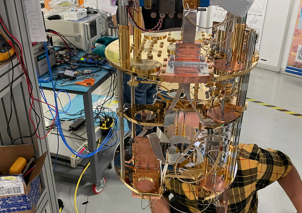
Fabrication of CMB-S4 prototype detector wafers is a key development goal for the project. The February newsletter highlighted the successful delivery of a first CMB-S4 prototype wafer produced by SEEQC/LBNL. This month we want to highlight ongoing work in our other wafer fabrication sites: NIST, JPL, UC Berkeley, and ANL.

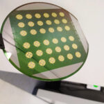
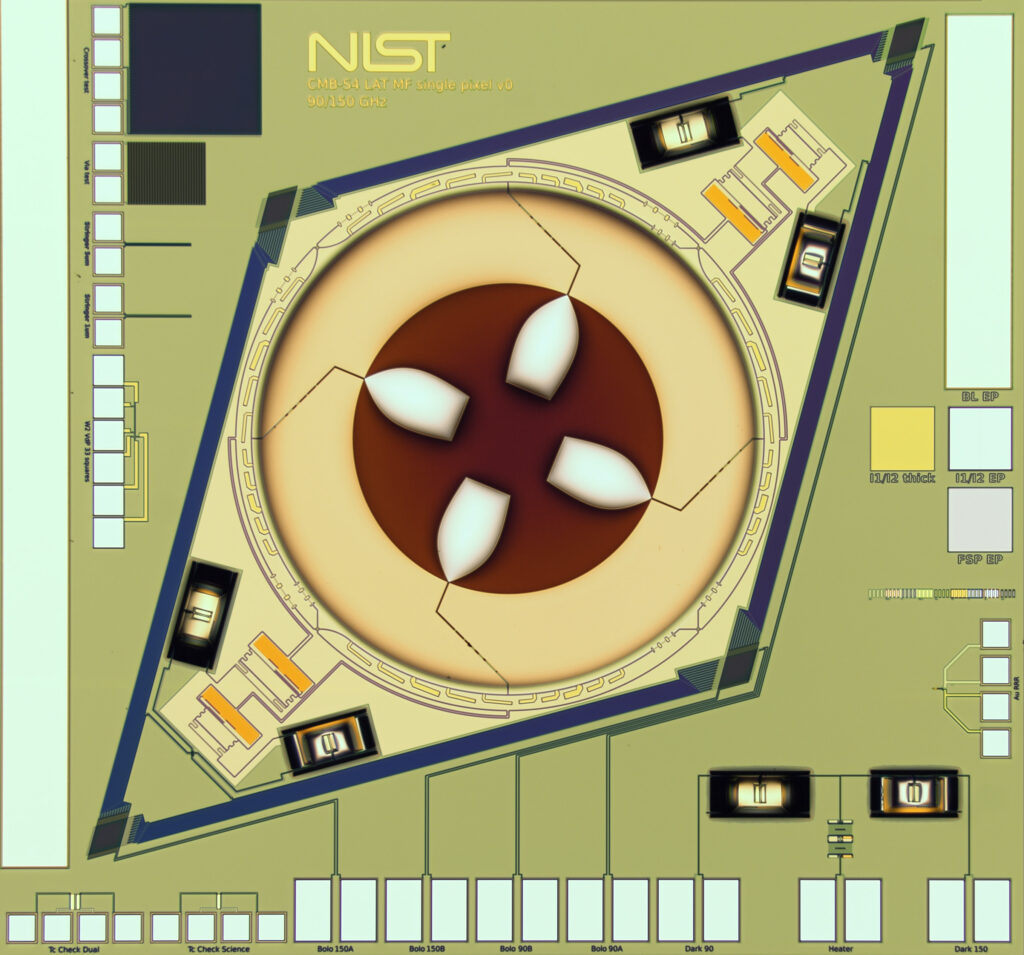
NIST is currently focused on building several single pixel test structures to validate detector design features. This modular approach enables precise optimization of fabrication conditions for the final wafer design. The completed test structures, see Fig. 1 (below: Microscope photo of a recently completed LAT mid-frequency prototype detector pixel at NIST. The superconducting circuit elements are clearly visible.) for a LAT mid-frequency pixel, are wirebonded to a circuit board that integrates into a cryostat for rapid testing at cryogenic temperatures.

Fig. 1: Microscope photo of a recently completed LAT mid-frequency prototype detector pixel at NIST. The superconducting circuit elements are clearly visible.

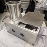
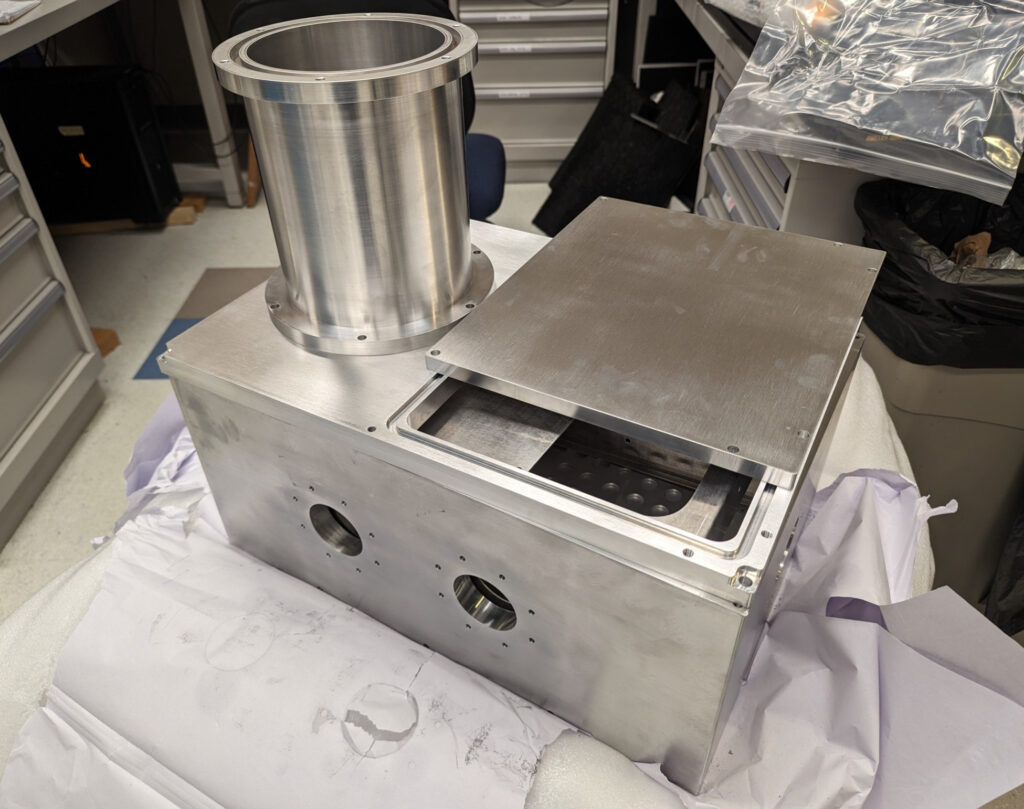
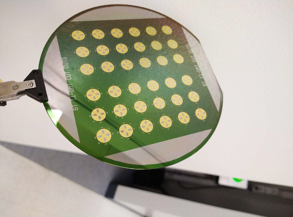
JPL completed the layout and mask design of a SAT mid-frequency single pixel, see Fig. 2, and a corresponding prototype wafer. JPL is making significant progress with validating their proposed fabrication steps by building and measuring properties of subcomponent structures. Parallel work has focused on optimizing the final, full wafer design to adapt to the fabrication capabilities at JPL.Fig. 2, below, is JPL’s recent design for the SAT mid-frequency detector pixel.

Fig. 2: JPL’s recent design for the SAT mid-frequency detector pixel.

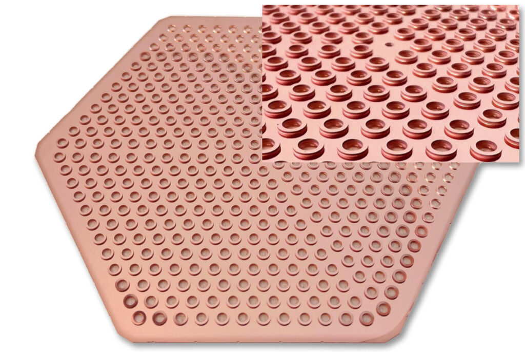
UC Berkeley’s development is focused on building low frequency detector wafers, which require large-diameter and free-standing nitride membranes to support the long-wave-length optimized OMT probes. Fig. 3, below, shows a test wafer successfully incorporating these fragile structures which is their most recent achievement. Support of the OMTs (Orthomode Transducers) – paddles coupling the CMB radiation to the detector RF circuits – requires large-diameter, free-standing, low-stress nitride membranes to hold the long-wave-length optimized OMT probes in place. UC Berkeley (with SEEQC support) has recently demonstrated this critical fabrication step.

Fig. 3: Support of the OMTs (Orthomode Transducers) - paddles coupling the CMB radiation to the detector RF circuits - requires large-diameter, free-standing, low-stress nitride membranes to hold the long-wave- length optimized OMT probes in place. UC Berkeley (with SEEQC support) has recently demonstrated this critical fabrication step.

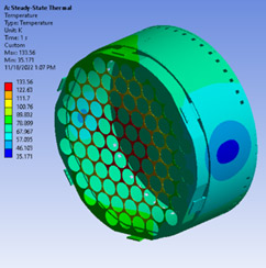
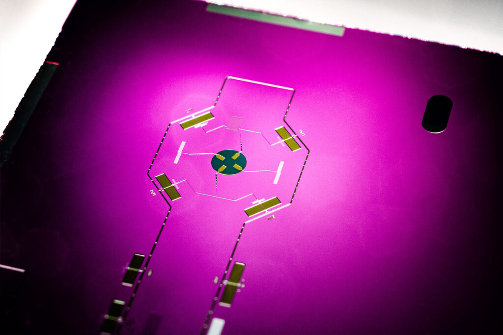
ANL concentrates effort on the development of the LAT mid-frequency wafers. Recent work has been focused on evaluating material properties using single pixel structures as shown in Fig. 4, below. ANL has validated material properties by carrying out systematic mm-wave loss studies of microstrip lines. The image shows a test setup with MKIDs and the microstrip line extending beyond the bottom of the photo. In addition, ANL is developing an optical test setup for rapid, cryogenic testing of single-pixel structures – similar to what has been developed at NIST.

Fig. 4: ANL has validated material properties by carrying out systematic mm-wave loss studies of microstrip lines. The image shows a test setup with MKIDs and the microstrip line extending beyond the bottom of the photo.


Key Dates and Upcoming Activities

Thanks for an exciting Spring Collaboration Meeting! The meeting focused on CMB-S4’s project baseline development after the recent conclusion of the Analysis of Alternatives. We heard about significant advancements developing the new project baseline (covering scientific, technical, simulation, and project management areas). The next Collaboration Meeting will be held in person at SLAC this summer – more details to follow.

  • CMB-S4 Summer Collaboration Meeting – week of July 31 – Aug 4, 2023


Originally posted in the CMB-S4 April 2023 Newsletter

Filed Under: newsfeed

Small Aperture Telescopes

March 22, 2023 by Matthaeus Leitner

CfA Optical Test Chamber

The Small Aperture Telescope (SAT) design team at CfA | Harvard & Smithsonian recently completed the assembly of a mini-cryostat for cryogenic testing of state-of-the-art optical materials to optimize the SAT telescope components. Fig. 5 (below) shows the newly fabricated vacuum chamber for the testing of optics components.

CfA Optical Test Chamber

In parallel, Berkeley Lab engineers continue to refine the design of the telescope focal plane and cryobus, especially in regards to integration with other sub-systems. Fig. 6, below, shows the SAT focal plane wiring design.

SAT Cryobus


Key Dates and Upcoming Activities

The project-focused Spring Collaboration Meeting is right around the corner. Please go to the meeting Indico page for more information. The meeting will be held remotely and registration is
required to receive a zoom link.

  • CMB-S4 Spring Collaboration Meeting – April 3 – 6, 2023
  • CMB-S4 Summer Collaboration Meeting – week of July 31 – Aug 4, 2023


Originally posted in the CMB-S4 March 2023 Newsletter 

Filed Under: newsfeed

Module Assembly and Testing

March 20, 2023 by Matthaeus Leitner

Fig. 2: A precision-etched LAT-MF waveguide interface plate made out of Cu coated silicon.

Fermilab is currently assembling components required to perform optical tests with the Large Aperture Telescope mid-frequency (LAT-MF) detector wafers.

Fig. 1, below, shows the Fermilab dilution refrigerator being prepared for testing detector modules. 100 mK electronics circuits have been installed recently, and Fermilab scientists are now preparing the choke, waveguide interface plate, and backshort wafers.

Fig. 1: Fermilab dilution refrigerator being prepared for testing detector modules.

These precision etched wafers hold the superconducting detector wafers in place and form a precisely shaped optical cavity for detecting the CMB microwave signal. Fig. 2, below, shows a recently completed precision-etched LAT-MF waveguide interface plate made out of Cu coated silicon. Radiation is coupled to the detector wafers through feedhorn arrays which are precision-machined to specific requirements of the telescope and its frequency band.

Fig. 2: A precision-etched LAT-MF waveguide interface plate made out of Cu coated silicon.

Fig. 3, below, shows a recently completed LAT-MF feedhorn array after inspection at Fermilab and the final gold-plating step. In addition, Fermilab’s engineering team has developed a novel feedhorn array configuration for the Small Aperture Telescopes (SAT).

Fig. 3: A recently completed LAT-MF feed-horn array after the final gold-plating step.

That design incorporates sloped sidewall corners to enable a tighter module packing for the curved SAT focal plane. Fig. 4, below, shows a newly developed compact feedhorn array design for the SAT curved focal plane.

Fig. 4: A newly developed compact feedhorn array design for the SAT curved focal plane.


Originally posted in the CMB-S4 March 2023 Newsletter 

Filed Under: newsfeed

Large Aperture Telescope Receiver Engineering

February 28, 2023 by Matthaeus Leitner

Thermal model of the LAT receiver cryostat. 2 of 2

The Large Aperture Telescope (LAT) receiver engineering group has developed a first thermal model of the 50 K radiation shield. Due to the large receiver size this sub-component is challenging to design. The shield supports the alumina IR filters which need to be sufficiently cooled. Several options are currently being investigated to reduce thermal gradients, e.g. improved heat straps or higher conductivity materials. The figures below show the thermal model of the LAT receiver cryostat.

Thermal model of the LAT receiver cryostat. 1 of 2

Thermal model of the LAT receiver cryostat. 2 of 2


Key Dates and Upcoming Activities

The project and collaboration have recently completed the Analysis of Alternatives. This allows us to refocus the project to developing a new project baseline for future reviews. We presented our strong and further strengthened science case to the P5 Particle Physics Project Prioritization Panel.

  • CMB-S4 Spring Collaboration Meeting – April 3 – 6, 2023
  • CMB-S4 Summer Collaboration Meeting – week of July 31 – Aug 4, 2023


Originally posted in the CMB-S4 February 2023 Newsletter

Filed Under: newsfeed

New Cold Load for Module Testing

February 24, 2023 by Matthaeus Leitner

cryogenic black-body cold load

Fermilab, SLAC, Washington University in St. Louis, and University of Illinois Urbana-Champaign have set up module test cryostats to qualify future CMB-S4 prototype wafers and module components including readout electronics. Fig. 1, below, shows a single wafer test cryostat (cryogenic black-body cold load). Fig. 2 shows Ian Gullett (Case Western) and Cesiley King (WashU) and a newly installed cold load, which is used to measure the optical efficiency of detector modules, at Washington University.

cryogenic black-body cold load

Newly installed cold load at Washington University.

Originally posted in the CMB-S4 February 2023 Newsletter

Filed Under: newsfeed

  • « Go to Previous Page
  • Go to page 1
  • Go to page 2
  • Go to page 3
  • Go to Next Page »

Copyright © 2025 · Parallax Pro CMB-S4 on Genesis Framework · WordPress · Log in